|
-
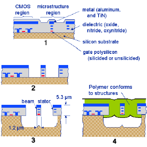
The chip comes from a standard CMOS
fabrication facility covered with a layer of
protective glass (silicon dioxide). Regions
meant for mechanical structures are
patterned in one of the metal layers, usually
the topmost layer.
-
The oxide is etched anisotropically
(directionally) down to the silicon substrate,
the metal layers acting as a mask to define
the mesh structure.
-
The underlying silicon substrate is etched
with an anisotropic deep etch followed by an
isotropic (all directions) etch to release the
metal-dielectric layers form the silicon
substrate underneath. At this point, the
membrane mesh structure is released from
the underlying silicon and the desired cavity
is formed. In the figure we see a
CMOS-MEMS beam (looking from the end),
and the metal layers inside which can be
used as electrodes for sensing and
actuation, or wires for connecting to the
on-chip circuitry.
-
In the final step, the released
CMOS-MEMS structure is coated with
polymer in a chemical vapor deposition
process. The polymer conforms to all sides
of the beams, until all the gaps are sealed,
creating an airtight membrane suspended
over the gap. The metal
layers inside the beams allow the membrane
to be treated as an electrode for either
capacitive sensing or electrostatic actuation.
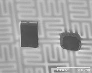
A scanning electron micrograph (SEM) of the mesh-polymer membrane.
Two holes have purposely been etched into the membrane to illustrate the mesh-membrane
structure and to reveal the cavity underneath the membrane.
In addition to the simple fabrication sequence, the
acoustic CMOS-MEMS devices have the
advantage of integrated, on-chip electronics. For
microphone applications, sensing circuitry
(capacitive or piezoresistive) can be placed close
to the mechanical structure, minimizing
electromagnetic pickup and parasitic
capacitance. For speaker applications, driver
circuitry can be placed nearby the mechanical
structures. In both microphone and speaker
applications, signal processing electronics for
signal conditioning (for example, noise
cancellation and equalization) are also on-chip,
increasing Akustica product performance,
reliability and affordability.
Demonstrated Devices
Acoustic CMOS-MEMS enables Akustica to
fabricate single and multiple membranes on
standard and state-of-the-art computer and signal
processing chips for revolutionary microphonic,
speaker or combined microphonic-speaker
applications addressing a variety of different
markets.
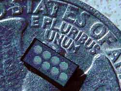
To date, acoustic CMOS MEMS have been used
to fabricate single-membrane earphone speakers
that are 2mm x 2mm square, a microphone less
than 1 mm x 1mm and speaker arrays with up to
eight (8) individually controllable speakers in an
area about twice the area of the eagle head on a
quarter.
Below is a picture of a 2 mm x 2 mm microphone
chip with a single membrane and integrated electronics.
The 0.7 mm x 0.7 mm membrane is the dark blue area in the
center with the associated and integrated electronics located
beneath the green rectangles distributed about the perimeter
of the chip.
The multi-membrane chip below is an array of eight
membranes, each individually controllable and electrically
isolated from the other membranes.
Array of eight octagonal speaker membranes.
|